|
STEP ATTENUATOR
Step Attenuator suitable for 0 - 30MHz.
Useful
for receiver sensitivity evaluations this Step Attenuator is a series
of switchable Pi attenuation pads as shown in Fig 1 schematic below.
The resistance values required were derived from paralleled on hand
resistors in stock. All
resistors are of a 5% tolerance however should be adequate for the
intended purpose. The
combination of step values were chosen as they represent values that
are easily for mental arithmetic however are not necessarily the most
efficient combination of values.
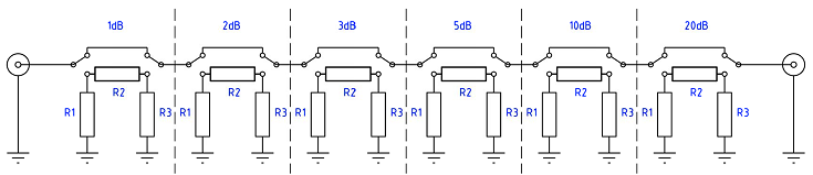
Fig
1 Step
Attenuator schematic. The broken lines represent PCB pad shielding.
| ATTENUATION
dB |
R1 |
R2 |
R3 |
| 1 |
869.55 |
5.7692 |
869.55 |
| 2 |
436.21 |
11.615 |
436.21 |
| 3 |
292.4 |
17.615 |
292.4 |
| 5 |
178.49 |
30.398 |
178.49 |
| 10 |
96.248 |
71.151 |
96.248 |
| 20 |
61.111 |
247.5 |
61.111 |
Fig
2
Attenuation pad resistor values.
| ATTENUATION
dB |
Resistors |
REQUIRED R |
Ra |
Rb |
PARALLEL
VALUE |
ERROR |
| 1 |
R1
& 3 |
869.55 |
1000 |
6800 |
871.795 |
-0.26% |
| R2 |
5.7692 |
6.8 |
39 |
5.790 |
-0.37% |
| 2 |
R1
& 3 |
436.21 |
680 |
1200 |
434.043 |
0.50% |
| R2 |
11.615 |
12 |
390 |
11.642 |
-0.23% |
| 3 |
R1
& 3 |
292.4 |
2700 |
330 |
294.059 |
-0.57% |
| R2 |
17.615 |
18 |
820 |
17.613 |
0.01% |
| 5 |
R1
& 3 |
178.49 |
180 |
22000 |
178.539 |
-0.03% |
| R2 |
30.398 |
33 |
390 |
30.426 |
-0.09% |
| 10 |
R1
& 3 |
96.248 |
150 |
270 |
96.429 |
-0.19% |
| R2 |
71.151 |
82 |
560 |
71.526 |
-0.53% |
| 20 |
R1
& 3 |
61.111 |
91 |
180 |
60.443 |
1.09% |
| R2 |
247.5 |
3300 |
270 |
249.580 |
-0.84% |
Fig
3 Resistor
combinations to achieve required attenuation pad resistor values.

Photo 1
Bottom rear view of the assembled Step Attenuator.

Photo 2
Top rear view of the assembled Step Attenuator.

Photo 3
Front view of the assembled Step Attenuator.

Fig
4 graph shows attenuation achieved at various frequencies.
The
graph in Fig 4 was derived from measuring the voltage applied to the
input against the voltage presented at the output at selected
frequencies. The results are applied to the below formula to calculate
the dB attenuation.


The
practical use of the step attenuator is to present a precise voltage reference
based on a known source voltage from a signal generator for example to
measure receiver sensitivity or calibrate receiver 'S' meter. The
below formula shown how to determine the output voltage from the step
attenuator with an input of 10mV with the attenuator set to -6dB
resulting in an output of 5.012mV.

V
= Voltage out
Vin
= Voltage input
The
below table gives a multiplier to apply to the
input voltage and derive the output for given dB attenuation. The formula
and the table are
for voltage only and not power.
|
dB
Attenuation
|
Attenuation
Multiplier
|
|
0
|
1
|
|
1
|
0.891250938
|
|
2
|
0.794328235
|
|
3
|
0.707945784
|
|
4
|
0.630957344
|
|
5
|
0.562341325
|
|
6
|
0.501187234
|
|
7
|
0.446683592
|
|
8
|
0.398107171
|
|
9
|
0.354813389
|
|
10
|
0.316227766
|
|
11
|
0.281838293
|
|
12
|
0.251188643
|
|
13
|
0.223872114
|
|
14
|
0.199526231
|
|
15
|
0.177827941
|
|
16
|
0.158489319
|
|
17
|
0.141253754
|
|
18
|
0.125892541
|
|
19
|
0.112201845
|
|
20
|
0.1
|
|
21
|
0.089125094
|
|
22
|
0.079432823
|
|
23
|
0.070794578
|
|
24
|
0.063095734
|
|
25
|
0.056234133
|
|
26
|
0.050118723
|
|
27
|
0.044668359
|
|
28
|
0.039810717
|
|
29
|
0.035481339
|
|
30
|
0.031622777
|
|
31
|
0.028183829
|
|
32
|
0.025118864
|
|
33
|
0.022387211
|
|
34
|
0.019952623
|
|
35
|
0.017782794
|
|
36
|
0.015848932
|
|
37
|
0.014125375
|
|
38
|
0.012589254
|
|
39
|
0.011220185
|
|
40
|
0.01
|
|
41
|
0.008912509
|
Fig
5 dB voltage multiplier table.
Related
projects:
Also
see step attenuator project: 40dB
Standard
Attenuator
References:
Pi
& Tee Network Resistive Attenuation Calculator
http://n9zia.ampr.org/att_pad.cgi
PI
Attenuator Calculator
http://www.random-science-tools.com/electronics/PI_attenuator.html
The
Pi-pad Attenuator - Equations
http://www.electronics-tutorials.ws/attenuators/pi-pad-attenuator.htm
Fixed
Pi and Tee Attenuators - Equations
http://www.rfcafe.com/references/electrical/attenuators.htm
TOP
OF PAGE
Page
last revised 12 March 2022
|